Siberian01
This board is based on the RP2040 microcontroller from the Raspberry Foundation.
It is a development board with the minimun requirements for the RP2040 IC to properly works, it complies with the USB 2.0 protocol, full use of all the GPIO pins, on board linear regulator for the 3.3V, 1 status led and another led connected to pin GPIO17.
It was designed with the purpose to learn how to design, assemble, document and manufacture (JLCPCB) printed circuit board (PCB’s).
SoC Features
- Dual ARM Cortex-M0+ @ 133MHz
- 264kB on-chip SRAM in six independent banks
- Support for up to 16MB of off-chip Flash memory via dedicated QSPI bus
- DMA controller
- Fully-connected AHB crossbar
- Interpolator and integer divider peripherals
- On-chip programmable LDO to generate core voltage
- 2 on-chip PLLs to generate USB and core clocks
- 30 GPIO pins, 4 of which can be used as analog inputs
- Peripherals:
- 2 UARTs
- 2 SPI controllers
- 2 I2C controllers
- 16 PWM channels
- USB 1.1 controller and PHY, with host and device support
- 8 PIO state machines
For the complete description of the microcontroller, see the RP2040 DATASHEET.
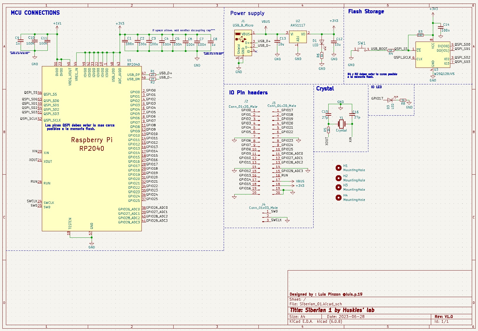 Schematic Diagram
Power
- USB Type B
Debug Pinout Connection
| Pin number | SoC | Description |
|---|---|---|
| 1 | 25 | SWD |
| 2 | – | GND |
| 3 | 24 | SWCLK |
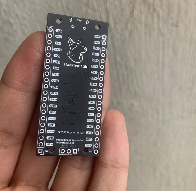
Pin Layout
Pin Layou pending…
Left Side
| Pin number | SoC | Description |
|---|---|---|
| 1 | 2 | GPIO0, SPI0 RX, UART0 TX, I2C0 SDA. |
| 2 | 3 | GPIO1, SPI0 CSn, UART0 RX, I2C0 SCL. |
| 3 | 4 | GPIO2, SPI0 SCK, UART0 CTS, I2C1 SDA. |
| 4 | 5 | GPIO3, SPI0 TX, UART0 RTS, I2C1 SCL. |
| 5 | 6 | GPIO4, SPI0 RX, UART1 TX, I2C0 SDA. |
| 6 | 7 | GPIO5, SPI0 CSn, UART1 RX, I2C0 SCL. |
| 7 | – | GND. |
| 8 | 8 | GPIO6, SPI0 SCK, UART1 CTS, I2C1 SDA. |
| 9 | 9 | GPIO7, SPI0 TX, UART1 RTS, I2C1 SCL. |
| 10 | 11 | GPIO8, SPI1 RX, UART1 TX, I2C0 SDA. |
| 11 | 12 | GPIO9, SPI1 CSn, UART1 RX, I2C0 SCL. |
| 12 | 13 | GPIO10, SPI1 SCK UART1 CTS I2C1 SDA. |
| 13 | 14 | GPIO11, SPI1 TX UART1 RTS I2C1 SCL. |
| 14 | – | GND. |
| 15 | 15 | GPIO12, SPI1 RX, UART0 TX, I2C0 SDA. |
| 16 | 16 | GPIO13, SPI1 CSn, UART0 RX, I2C0 SCL. |
| 17 | 17 | GPIO14, SPI1 SCK, UART0 CTS, I2C1 SDA. |
| 18 | 18 | GPIO15, SPI1 TX, UART0 RTS, I2C1 SCL. |
| 19 | 27 | GPIO16, SPI0 RX, UART0 TX, I2C0 SDA. |
| 20 | – | GND. |
Right Side
| Pin number | SoC | Description |
|---|---|---|
| 21 | 28 | GPIO17, SPI0 CSn, UART0 RX, I2C0 SCL. |
| 22 | 29 | GPIO18, SPI0 SCK, UART0 CTS, I2C1 SDA. |
| 23 | 30 | GPIO19, SPI0 TX, UART0 RTS, I2C1 SCL. |
| 24 | 31 | GPIO20, SPI0 RX, UART1 TX, I2C0 SDA, CLOCK GPIN0. |
| 25 | 32 | GPIO21, SPI0 CSn, UART1 RX, I2C0 SCL, CLOCK GPOUT0. |
| 26 | 34 | GPIO22, SPI0 SCK, UART1 CTS, I2C1 SDA,CLOCK GPIN1. |
| 27 | – | GND. |
| 28 | 35 | GPIO23, SPI0 TX, UART1 RTS, I2C1 SCL, CLOCK GPOUT1. |
| 29 | 36 | GPIO24, SPI1 RX, UART1 TX, I2C0 SDA, CLOCK GPOUT2. |
| 30 | 36 | GPIO25, SPI1 CSn, UART1 RX, I2C0 SCL, CLOCK GPOUT3. |
| 31 | 38 | GPIO26_ADC0, SPI1 SCK, UART1 CTS, I2C1 SDA. |
| 32 | 39 | GPIO27_ADC1, SPI1 TX, UART1 RTS, I2C1 SCL. |
| 33 | 40 | GPIO28_ADC2, SPI1 RX, UART0 TX, I2C0 SDA. |
| 34 | – | GND. |
| 35 | 41 | GPIO29_ADC3,SPI1 CSn, UART0 RX, I2C0 SCL. |
| 36 | 26 | RUN |
| 37 | – | VBUS |
| 38 | – | +3V3 |
| 39 | – | GND. |
| 40 | – | GND. |
| Function | SoC |
|---|---|
| SPIx. | Connect one of the internal PL022 SPI peripherals to GPIO. |
| UARTx. | Connect one of the internal PL011 UART peripherals to GPIO. |
| I2Cx. | Connect one of the internal DW I2C peripherals to GPIO. |
| CLOCK GPINx. | General purpose clock inputs. Can be routed to a number of internal clock domains on RP2040, e.g. to provide a 1Hz clock for the RTC, or can be connected to an internal frequency counter. |
| CLOCK GPOUTx. | General purpose clock outputs. Can drive a number of internal clocks (including PLLoutputs) onto GPIOs, with optional integer divide. |
Board Design
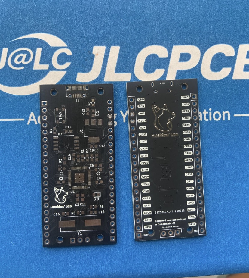
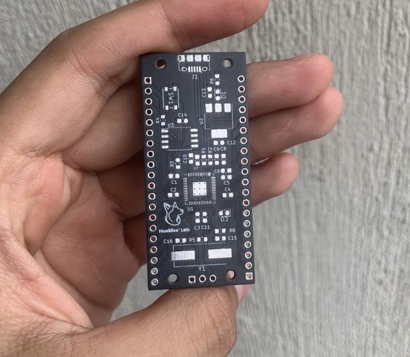
Top
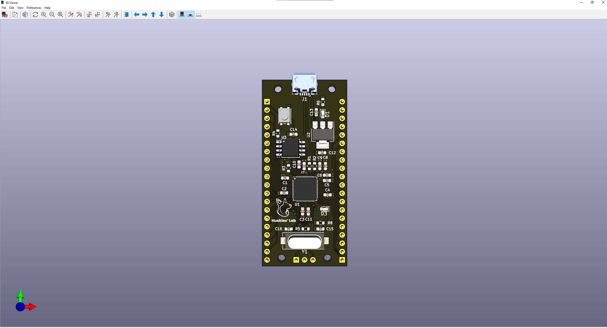 Top View
Bottom
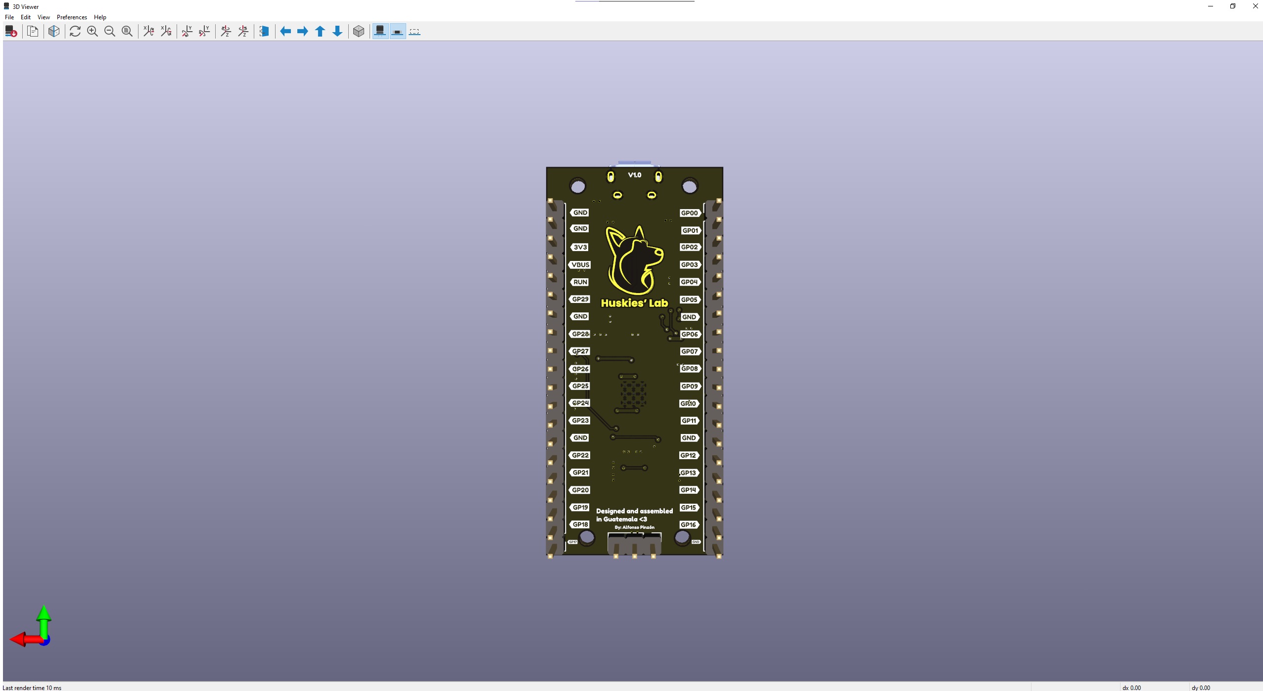 Botton View
Bill of Material
Status of the project.
At this moment I have received the boards from JLCPCB, but I have not assembled them just yet, I’m still witing the components from China, but once I get them I can start the process to assamble and test the functionality of the board and confirm if there are errors or not, and if a v2.0 would be needed.